Chiplet Visibility: Mapping the Inside of a SiP
The semiconductor industry is rapidly shifting toward Systems‑in‑Package (SiP) designs that integrate multiple chiplets into a single module. This trend is driven by demand from cloud data centers, telecom networks, smartphones, automotive electronics, and high‑performance computing. As companies move away from monolithic chips, advanced packaging techniques become essential for delivering the performance and reliability required by next‑generation AI workloads.
Breaking news
 Canonical’s Web Presence Hit by Second DDoS Assault This Year
 Loops AI Secures $3.5 Million to Power a New AI Operating System for E‑Commerce
 Winverse AI Secures Tens of Millions in Seed Funding from DeepSeek and Long‑Z
 Google Adds Pixel 9 Series to Certified Refurbished Store
Advanced packaging enables heterogeneous integration, allowing processors, memory, and specialized accelerators to coexist on a compact substrate. By stacking and interconnecting chiplets with fine‑pitch interposers, manufacturers can tailor each component to its optimal technology node, reducing power consumption and latency. The approach also simplifies thermal management, as heat can be spread across the package rather than concentrated in a single die. Industry analysts estimate that SiP adoption could boost overall system efficiency by up to 30 % compared with traditional multi‑chip solutions.
Understanding every chiplet inside a SiP is no longer a theoretical exercise. Engineers now employ high‑resolution X‑ray tomography and machine‑learning‑driven inspection tools to create detailed maps of each component’s placement, interconnect density, and electrical characteristics. „We can now see the exact routing of signals between a GPU die and a high‑bandwidth memory stack,” said Dr. Lena Wu, senior packaging architect at a leading fab. This visibility helps identify potential failure points early, allowing designers to adjust layout before costly tape‑out stages. Moreover, real‑time monitoring embedded in the package can report temperature, voltage, and signal integrity metrics, feeding data back to system‑level management software for dynamic performance tuning.
Will Advanced Packaging Accelerate AI Deployment in Edge Devices?
The answer appears to be yes. Edge computing platforms, from autonomous vehicles to smart cameras, require AI inference at low latency while operating under strict power budgets. Advanced packaging delivers the necessary bandwidth by placing AI accelerators directly next to memory, eliminating the bottlenecks of traditional board‑level connections. Recent prototypes demonstrate that a SiP‑based vision processor can process 4K video streams at 120 fps while consuming less than 8 watts—figures unattainable with discrete components. This capability is prompting OEMs to redesign product roadmaps, integrating SiP modules as core building blocks rather than optional add‑ons.
The shift toward advanced packaging reshapes the semiconductor supply chain. Foundries must invest in new lithography and bonding equipment, while design houses need expertise in multi‑die verification. As the ecosystem matures, costs are expected to decline, making SiP solutions viable for mid‑range products as well as premium offerings. In the long term, the ability to mix and match chiplets could spur rapid innovation cycles, allowing manufacturers to upgrade individual functions without redesigning entire systems.
Frequently Asked Questions
What distinguishes a System‑in‑Package from a traditional multi‑chip module? A SiP integrates multiple chiplets on a single substrate with high‑density interconnects, offering tighter coupling, lower latency, and better thermal distribution than board‑level multi‑chip assemblies.
How does advanced packaging improve AI performance? By placing compute engines next to memory and using ultra‑fast interposers, SiPs reduce data movement delays, enabling faster inference and lower power consumption for AI workloads.
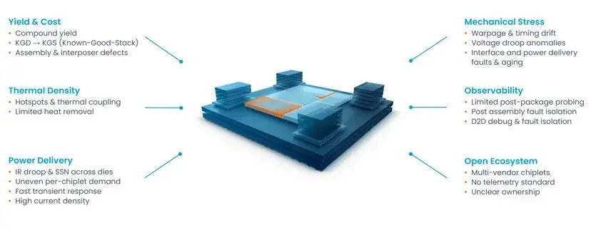
Are there any challenges associated with adopting advanced packaging? Key hurdles include the need for specialized manufacturing equipment, complex design verification across heterogeneous dies, and ensuring long‑term reliability of densely packed interconnects.