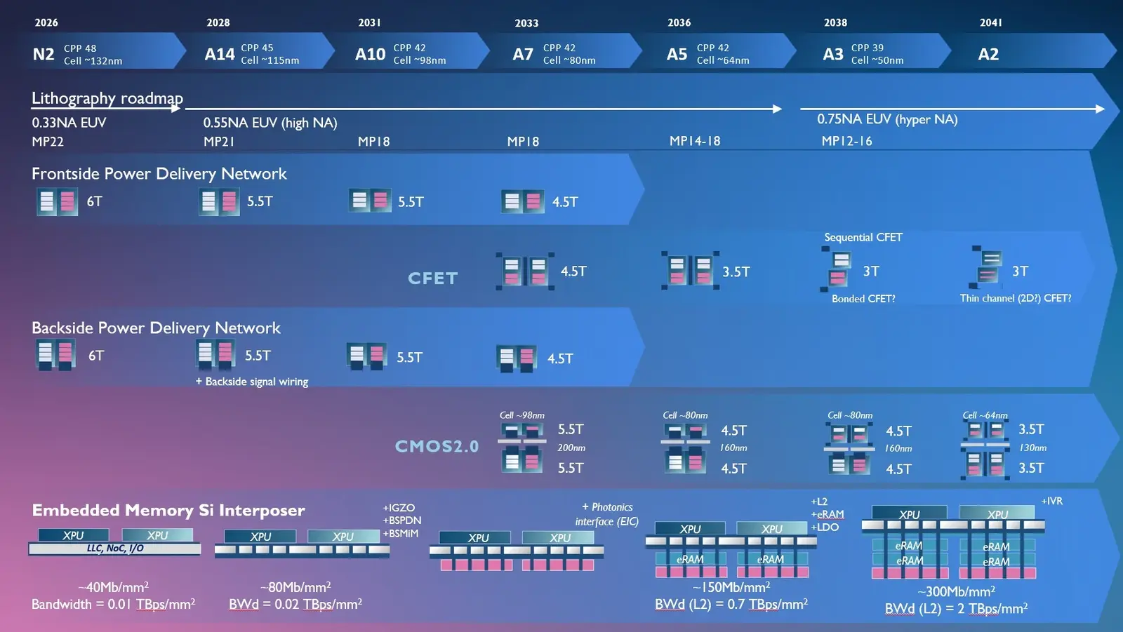
Split‑Gate Design: A New Standard Cell Architecture
A recent industry briefing highlighted a shift toward CFET‑based transistor architectures starting with the A7 logic node. Companies are moving to 4.5‑track and smaller standard cells, driven by the promise of higher density and lower power consumption. The transition is supported by two research tracks, with imec leading many of the core innovations.
Breaking news
 Town AI Secures $108 Million Series B, Valued at $1 Billion After $55 M Pre‑Series
 Apple Prepares for Major Product Launch Event on October 28
 Apple Releases Release Candidates for watchOS, tvOS and visionOS 27.2
 Apple Limits iPhone Duo and iPhone 18 Pro Max to Reservation-Only Sales in Japan and South Korea
The briefing explained that CFETs—channel‑length‑modulated field‑effect transistors—allow designers to reduce the number of transistors per cell without sacrificing performance. By splitting the gate structure, engineers can create a 5T+1 CFET SRAM bit that fits into a 4.5‑track layout. This new cell design maintains data integrity while cutting area by roughly 15 percent compared to conventional 6T cells. The reduced footprint also lowers leakage currents, a critical factor for mobile and IoT devices.
The split‑gate approach divides the gate electrode into two segments, each controlling a different portion of the channel. This configuration enables independent tuning of threshold voltage and drive current for the two halves. As a result, the cell can operate with fewer transistors while still meeting speed and noise margins required by modern logic. imec’s prototype demonstrated a 10‑percent improvement in drive strength at the same supply voltage, indicating that the new architecture does not compromise performance.
Will CFETs Replace Traditional Transistors in the Near Future?
Industry analysts noted that the 5T+1 CFET SRAM cell could be integrated into existing design flows with minimal changes. The cell’s compatibility with standard fabrication processes means that foundries can adopt the technology without extensive retooling. This ease of integration is a key factor driving the expected industry uptake.
Experts predict that CFETs will become mainstream by the late 2020s, especially in high‑density memory and low‑power logic. The technology’s ability to shrink cell size while keeping power consumption low aligns with the semiconductor industry's push toward smaller nodes. However, challenges remain, such as ensuring uniformity across large wafers and managing the increased complexity of gate fabrication. Continued collaboration between device manufacturers and research institutions will be essential to overcome these hurdles.
The long‑term impact of CFET adoption could be significant. Smaller, faster cells will enable more powerful processors in compact form factors, benefiting everything from smartphones to edge computing devices. Additionally, the reduced power draw could extend battery life and lower operational costs for data centers.
Frequently Asked Questions
What is a CFET and how does it differ from a conventional transistor? A CFET, or channel‑length‑modulated field‑effect transistor, uses a split‑gate structure to control different sections of the channel independently. This allows for smaller cell sizes and lower leakage compared to traditional transistors.
How does the 5T+1 CFET SRAM cell improve upon the standard 6T design? The 5T+1 design removes one transistor while adding a CFET, reducing area by about 15 % and cutting leakage currents, all while maintaining comparable speed and stability.
When can we expect CFETs to be widely available in commercial products? Industry forecasts suggest mainstream adoption by the late 2020s, once fabrication challenges are addressed and foundries incorporate the technology into their production lines.