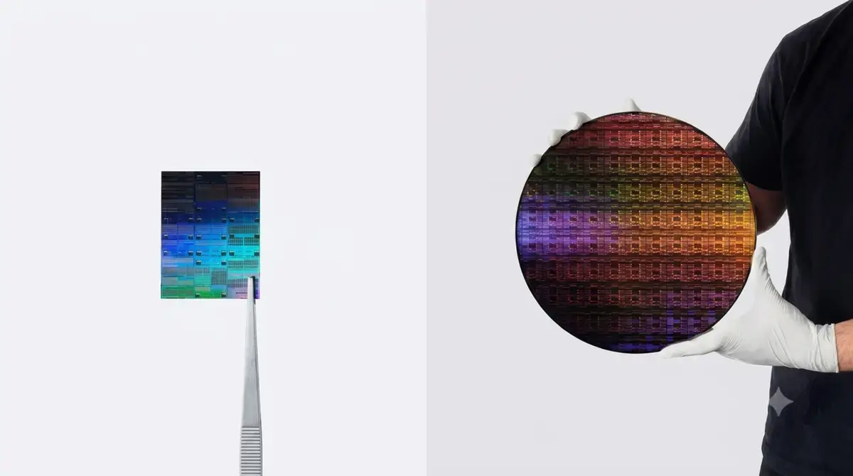
A Skyscraper of Transistors
IBM has unveiled a revolutionary 0.7 nm chip, dubbed NanoStack, packing 100 billion transistors in a tiny footprint. The breakthrough was announced on June 29, 2026. This innovative design achieves unprecedented processing power density.
Breaking news
 Canonical’s Web Presence Hit by Second DDoS Assault This Year
 Loops AI Secures $3.5 Million to Power a New AI Operating System for E‑Commerce
 Winverse AI Secures Tens of Millions in Seed Funding from DeepSeek and Long‑Z
 Google Adds Pixel 9 Series to Certified Refurbished Store
The NanoStack design stacks transistors in a three-dimensional structure, much like a 100-storey skyscraper, to maximize efficiency. This ambitious approach enables the chip to deliver immense processing capabilities while minimizing its physical size.
Can This Technology Be Scaled?
The NanoStack chip's unique architecture allows it to accommodate an enormous number of transistors, far exceeding those found in entire data centers. By stacking transistors, IBM has effectively increased processing power without expanding the chip's footprint. This design is a significant departure from traditional chip design.
The 0.7 nm NanoStack chip represents a major milestone in chip development, demonstrating the feasibility of extremely dense transistor packing. Experts liken the design to a high-rise building, where each floor represents a layer of transistors.
As IBM pushes the boundaries of chip design, the question remains whether this technology can be scaled for mass production. The company's achievement is a significant step forward, but it also raises concerns about manufacturing complexity and cost.
Frequently Asked Questions
The implications of this breakthrough are far-reaching, with potential applications in fields like artificial intelligence, data analytics, and cloud computing. As the industry adopts this technology, we can expect significant advancements in processing power and efficiency.
What is the NanoStack chip? The NanoStack chip is a revolutionary 0.7 nm chip design that packs 100 billion transistors in a tiny footprint. It achieves this through a three-dimensional stacking structure. How does the NanoStack design work? The design stacks transistors in a 3D structure, maximizing processing power density. What are the potential applications of this technology? The NanoStack chip has potential applications in fields like artificial intelligence, data analytics, and cloud computing, where high processing power is required.