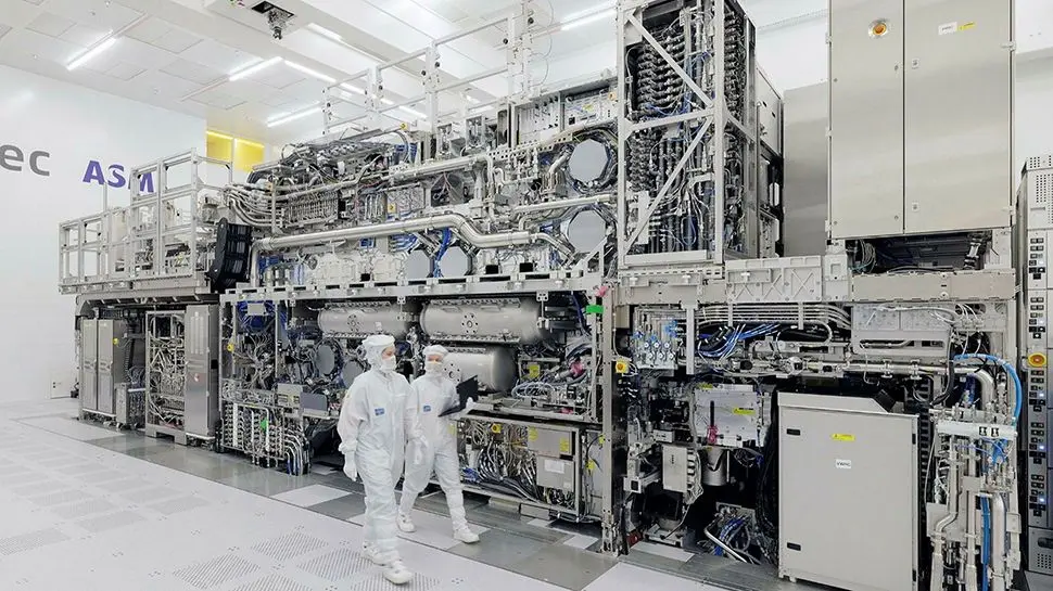
How Intel scaled High-NA EUV production so quickly
Intel announced it has processed over one million wafers using high-numerical-aperture extreme ultraviolet lithography, a milestone reached as of September 2026. This volume represents approximately three-quarters of all High-NA EUV wafers exposed globally to date. The achievement underscores Intel's aggressive adoption of next-generation chipmaking technology ahead of broader industry uptake.
Breaking news
 Town AI Secures $108 Million Series B, Valued at $1 Billion After $55 M Pre‑Series
 Apple Prepares for Major Product Launch Event on October 28
 Apple Releases Release Candidates for watchOS, tvOS and visionOS 27.2
 Apple Limits iPhone Duo and iPhone 18 Pro Max to Reservation-Only Sales in Japan and South Korea
The company's early and sustained investment in ASML's High-NA EUV systems has allowed it to run volume production on the tool while many competitors remain in pilot or development phases. Intel's internal data shows its wafer throughput now exceeds the combined total of all other semiconductor manufacturers using the technology. This head start is tied to Intel's strategy of de-risking future process nodes by securing early access to advanced lithography.
What does this mean for the future of chip manufacturing?
Intel's success stems from close collaboration with ASML during the tool's development, including early engineering samples installed at its Oregon and Arizona sites. The company optimized its 18A process node specifically around High-NA EUV capabilities, enabling tighter transistor scaling and improved performance per watt. Engineers report yield improvements of over 20% compared to previous-generation EUV tools at equivalent volumes. Internal training programs accelerated technician proficiency, reducing tool downtime and increasing throughput. Intel also adjusted its fab logistics to prioritize High-NA EUV lines, treating them as critical path assets rather than experimental equipment.
This milestone suggests Intel may maintain a process technology lead through the middle of the decade, particularly in logic and advanced packaging. Competitors like TSMC and Samsung are expected to reach similar wafer volumes by late 2027, but Intel's early experience could translate into better design rules and lower defect rates. Analysts note that volume familiarity with High-NA EUV is as critical as the hardware itself, giving Intel a potential edge in timing future nodes like 14A and 10A. The company plans to expand High-NA EUV capacity across its Fab 34 in Ireland and Fab 52 in Arizona by 2028.
How many High-NA EUV wafers has the rest of the industry processed combined? The rest of the industry has processed fewer than one million High-NA EUV wafers in total, meaning Intel's output exceeds the combined volume of all other manufacturers.
Frequently Asked Questions
Why is High-NA EUV important for future chip development? High-NA EUV enables finer circuit patterns than previous lithography tools, allowing for higher transistor density and improved performance, which is essential for advancing beyond the 2nm process node.
Is Intel sharing its High-NA EUV expertise with partners or foundry clients? Intel has not indicated plans to share its High-NA EUV process know-how externally; the knowledge remains internal to support its own integrated device manufacturing roadmap.