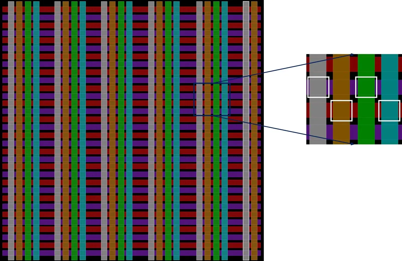
Enhancing Signal Integrity in Dense Architectures
Semiconductor engineers are adopting automated via insertion to overcome critical interconnect bottlenecks in sub-5nm chip designs. As transistor density increases, traditional wiring methods struggle to maintain performance. This new methodology improves signal integrity and power efficiency, ensuring that modern system-on-chip architectures meet the rigorous demands of advanced computing environments.
Breaking news
 Town AI Secures $108 Million Series B, Valued at $1 Billion After $55 M Pre‑Series
 Apple Prepares for Major Product Launch Event on October 28
 Apple Releases Release Candidates for watchOS, tvOS and visionOS 27.2
 Apple Limits iPhone Duo and iPhone 18 Pro Max to Reservation-Only Sales in Japan and South Korea
Designers currently face significant hurdles as interconnect delays surpass gate delays in modern silicon. The complexity of routing billions of transistors requires precise control over physical layout. Automated tools now insert redundant vias strategically, which mitigates the risk of manufacturing defects and enhances the overall durability of the chip’s internal wiring networks.
The shift toward smaller nodes forces a re-evaluation of how electrical signals travel across a die. By utilizing algorithmic via placement, engineers can reduce resistance and parasitic capacitance. These improvements are essential for maintaining high clock speeds without exceeding strict power consumption limits. Automated insertion eliminates human error during the tedious manual routing process.
Can Automated Routing Solve the Interconnect Crisis?
Furthermore, this technique provides a robust defense against localized thermal stress. By distributing the electrical load across multiple pathways, the risk of electromigration is significantly lowered. This structural resilience ensures that high-performance processors remain functional over longer lifespans, even when operating under heavy computational loads in constrained physical spaces.
The industry is betting heavily on automation to solve the physical design bottleneck. While manual layout was once the standard, the sheer scale of sub-5nm chips makes it impossible to optimize by hand. Automated via insertion acts as a force multiplier, allowing design teams to focus on high-level architecture while the software handles the microscopic wiring challenges.
Frequently Asked Questions
Looking ahead, the integration of these tools will likely become a mandatory step for all advanced node developments. As manufacturers push toward even smaller dimensions, the precision offered by automated systems will define the next generation of hardware. This transition marks a fundamental change in how we approach the physical realization of complex digital systems.
Why is via insertion critical for sub-5nm chips? As transistors shrink, the wiring connecting them becomes the primary source of performance degradation. Automated via insertion optimizes these connections to prevent signal loss and power waste.
How does automation improve manufacturing reliability? Automated tools consistently apply design rules that minimize the risk of electrical shorts or open circuits. This leads to higher production yields and more durable final products.