Mastering the Complexity of Vertical Stacking
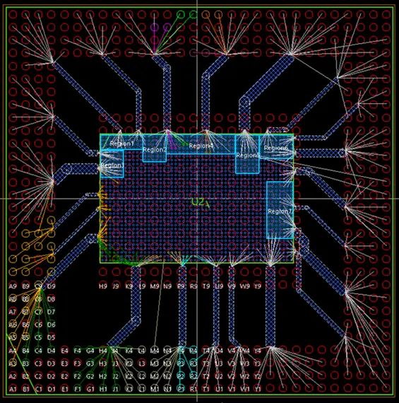
The semiconductor industry is rapidly shifting toward 3D-IC architectures to achieve superior performance and compact form factors. By vertically stacking active device layers connected through silicon vias, engineers are overcoming the limitations of traditional 2D designs. This transition requires meticulous attention to substrate implementation to ensure reliable power delivery and signal integrity.
Breaking news
 Town AI Secures $108 Million Series B, Valued at $1 Billion After $55 M Pre‑Series
 Apple Prepares for Major Product Launch Event on October 28
 Apple Releases Release Candidates for watchOS, tvOS and visionOS 27.2
 Apple Limits iPhone Duo and iPhone 18 Pro Max to Reservation-Only Sales in Japan and South Korea
Vertical integration allows manufacturers to pack more functionality into smaller spaces. However, this complexity creates significant hurdles during the finalization and tapeout phases. Designers must balance thermal management with electrical performance to prevent system failures. Effective substrate planning is now the cornerstone of modern chip development, directly influencing the success of high-density electronic products.
Standard 2D manufacturing relies on lateral spacing, but 3D-ICs demand precise vertical alignment. Through-silicon vias serve as the vital pathways for data and power between stacked layers. If these connections are not perfectly optimized, signal degradation can compromise the entire device. Engineers must simulate these interactions early in the design cycle to avoid costly errors.
Can Modern Design Tools Keep Pace with 3D Demands?
The transition to 3D structures also changes how power is distributed across the chip. Because heat dissipation is more difficult in a stacked environment, the substrate must act as an efficient thermal conduit. Designers are increasingly using advanced materials to improve conductivity. These technical refinements are essential for maintaining the performance gains promised by 3D technology.
The shift toward 3D-IC designs forces a complete overhaul of traditional tapeout workflows. Current software must handle multi-die interactions that were previously non-existent in 2D layouts. Without integrated platforms that manage substrate and die-to-die connectivity simultaneously, the risk of design flaws increases exponentially. Industry leaders are focusing on unified environments to streamline this transition.
Frequently Asked Questions
As the industry moves forward, the ability to finalize these complex designs efficiently will determine market leadership. Companies that master substrate integration will enjoy faster time-to-market and higher yields. While the challenges of vertical stacking remain steep, the potential for smaller, more powerful devices continues to drive intense innovation in the semiconductor sector.
What makes 3D-IC design more difficult than 2D design? 3D-IC design requires managing vertical connectivity through silicon vias and complex thermal dissipation. These factors create new challenges for signal integrity and power delivery that do not exist in flat 2D layouts.
Why is substrate implementation critical for tapeout? The substrate serves as the foundation for the entire stacked architecture. If the substrate is not properly finalized, the device may suffer from electrical interference or overheating, leading to a failed tapeout.