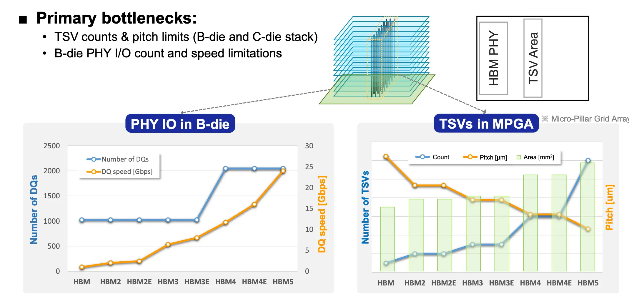
The Engineering Limits of Vertical Stacking
Engineers are encountering severe physical roadblocks as they attempt to stack more layers into High Bandwidth Memory (HBM). During the recent Hot Chips conference, industry experts highlighted how thinner dies and complex thermal management are straining manufacturing capabilities. This technical bottleneck arrives as AI companies demand faster data movement, putting immense pressure on global DRAM suppliers.
Breaking news
 Town AI Secures $108 Million Series B, Valued at $1 Billion After $55 M Pre‑Series
 Apple Prepares for Major Product Launch Event on October 28
 Apple Releases Release Candidates for watchOS, tvOS and visionOS 27.2
 Apple Limits iPhone Duo and iPhone 18 Pro Max to Reservation-Only Sales in Japan and South Korea
The push for increased bandwidth requires manufacturers to pack more capacity into smaller footprints. This transition necessitates larger Through-Silicon Via (TSV) areas, which complicates the assembly process. As layers grow thinner to maintain vertical height, the risk of structural failure and heat dissipation issues rises significantly. These physical constraints are driving up production costs and limiting overall industry output.
Manufacturers are struggling to balance performance gains with the realities of silicon physics. Each additional layer increases the complexity of the signal path and thermal output. Because AI workloads generate massive amounts of heat, managing the thermal profile of these dense memory stacks has become a primary concern for designers.
Can Manufacturers Overcome the Capacity Crunch?
Current fabrication methods are reaching their limits regarding how thin a die can be safely sliced. When dies become too fragile, yields drop, leading to higher prices for end users. The industry is currently trapped in a cycle where the demand for more memory capacity directly conflicts with the physical durability of modern DRAM components.
The ongoing shortage of DRAM is not merely a supply chain issue but a fundamental manufacturing crisis. As the big three DRAM vendors scramble to meet system-level requirements, the entire semiconductor ecosystem feels the strain. If these companies cannot stabilize production yields, the rapid expansion of AI infrastructure could face significant delays in the coming years.
Frequently Asked Questions
The future of HBM depends on breakthroughs in material science and packaging technology. Without new methods to dissipate heat and improve structural integrity, the pace of memory scaling will likely decelerate. Industry leaders must now decide whether to prioritize raw capacity or invest in more reliable, lower-density architectures.
Why is HBM scaling becoming more difficult? Scaling is limited by the physical fragility of thinner dies and the extreme heat generated by dense memory stacks. These factors make manufacturing more complex and prone to errors.
How does this affect the broader chip industry? The shortage of high-performance DRAM creates a bottleneck for AI systems. This scarcity drives up costs and slows the deployment of advanced computing hardware across the global market.