This collaborative model reduces risk and cost for partners developing
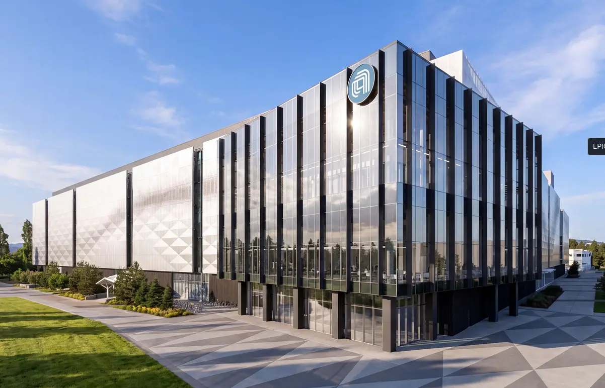
Applied Materials Inc. opened its new Equipment and Process Innovation and Commercialization Center on October 12, 2026, in Santa Clara, California. The $5 billion facility spans over 1 million square feet and brings together engineers, researchers, and industry partners under one roof to accelerate chip development. This launch marks one of the largest private investments in semiconductor R&D in recent years. The center focuses on advancing process innovation, equipment design, and commercialization pathways for next-generation semiconductors. By integrating R&D with pilot production capabilities, Applied Materials aims to shorten the time from lab breakthrough to factory deployment. The facility supports work on advanced nodes, chiplet architectures, and materials science critical for AI and high-performance computing. How the Facility Enables Faster Innovation Cycles The center includes shared labs where customers and equipment makers can test new processes in real time using Applied’s latest tools.
Breaking news
 Chinese Firms Secure Over One Million Nvidia Graphics Cards for AI Development
 Accenture Market Cap Surges to $130B Ahead of Investor Day
 Paris Startup Naboo Rebrands to Target Finance and Procurement Teams
 Improving Data Integrity in Automated Document Processing
This collaborative model reduces risk and cost for partners developing cutting-edge chips. Engineers can iterate on designs quickly, leveraging data from integrated metrology and AI-driven process control systems housed within the facility. What Role Will This Play in U. S. Semiconductor Leadership? Applied Materials says the center strengthens domestic innovation capacity amid global competition for chip supremacy. It aligns with federal incentives aimed at boosting U. S. semiconductor manufacturing and research. The company expects the hub to attract talent and foster partnerships that keep American firms at the forefront of technological advancement. Frequently Asked Questions What types of chips will be developed at the new facility? The center will focus on logic, memory, and advanced packaging technologies for applications in AI, data centers, and mobile devices, with emphasis on nodes below 2nm. How does this investment compare to previous Applied Materials R&D efforts?
At $5 billion, this single facility exceeds the company’s total annual R&D spending in recent years, representing a major escalation in its commitment to innovation leadership. Will the facility be open to external researchers and startups? Yes, Applied Materials plans to collaborate with universities, startups, and established chipmakers through joint development programs and shared access to select tools and labs.