Integrated Metrology: A Multilayered Shield
In the world of advanced semiconductor packaging, each layer and every process step adds value to a product. By the time chiplets, high‑bandwidth memory stacks, or hybrid‑bonded devices reach the final assembly stage, manufacturers have poured significant resources into them. A single unnoticed flaw at this point can jeopardise the entire investment, leading to costly recalls or warranty claims.
Breaking news
 Canonical’s Web Presence Hit by Second DDoS Assault This Year
 Loops AI Secures $3.5 Million to Power a New AI Operating System for E‑Commerce
 Winverse AI Secures Tens of Millions in Seed Funding from DeepSeek and Long‑Z
 Google Adds Pixel 9 Series to Certified Refurbished Store
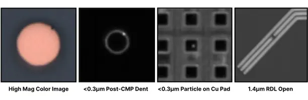
The challenge lies in detecting tiny defects that can slip past conventional inspection methods. Traditional optical or X‑ray systems often miss sub‑micron anomalies or fail to differentiate between harmless artefacts and genuine failures. To address this, industry leaders are combining complementary metrology techniques—such as laser‑based profilometry, electrical testing, and advanced imaging—to create a more robust defect‑detection framework.
By layering multiple inspection tools, manufacturers can cross‑verify findings and reduce false positives. For example, a laser profilometer may flag a surface irregularity, while an electrical probe confirms whether that irregularity interferes with signal integrity. This dual‑verification approach sharpens the accuracy of defect identification, allowing engineers to isolate true defects from benign variations.
Can Early Detection Cut Costs Dramatically?
The integration also speeds up the process. Rather than routing a wafer through separate inspection stages, a unified system can perform several tests in a single pass. This consolidation cuts down on handling time and reduces the risk of introducing new defects during transfer.
Early detection is not just a quality‑control exercise; it’s a financial strategy. A study by a leading semiconductor research firm found that detecting a defect before final assembly can save up to 30 % of the cost associated with a late‑stage failure. The savings come from avoiding re‑work, reducing scrap rates, and protecting brand reputation.
Moreover, the data gathered from integrated inspections feed into machine‑learning models that predict defect likelihood in future batches. This predictive capability enables proactive process adjustments, further lowering defect rates and enhancing yield.
The Human Element: Training and Expertise
While advanced tools provide powerful insights, they require skilled operators to interpret results accurately. Companies are investing in specialized training programs that blend engineering knowledge with data‑analysis skills. These programs help technicians distinguish between genuine defects and benign artefacts, ensuring that the inspection pipeline remains efficient and reliable.
The shift toward data‑driven quality control also means that engineers must stay current with evolving algorithms and sensor technologies. Continuous learning is becoming a core competency in the semiconductor industry, as the pace of innovation keeps accelerating.
The consequence of failing to catch defects early is a domino effect: increased warranty costs, supply‑chain disruptions, and erosion of customer trust. By contrast, a robust, integrated inspection strategy can safeguard investments, improve yields, and position companies for long‑term success in a highly competitive market.
Frequently Asked Questions
What types of defects are most critical in hybrid bonding? Bonding defects such as voids, misalignments, or contamination can severely impact electrical performance and reliability, making them top priorities for detection.
How does integrated metrology improve yield? By combining multiple inspection methods, manufacturers reduce false positives and catch defects earlier, leading to higher yields and lower re‑work costs.
Is the investment in integrated inspection justified for small manufacturers? Yes. Even smaller fabs can benefit from modular inspection systems that scale with production volumes, providing cost‑effective defect detection and yield improvement.