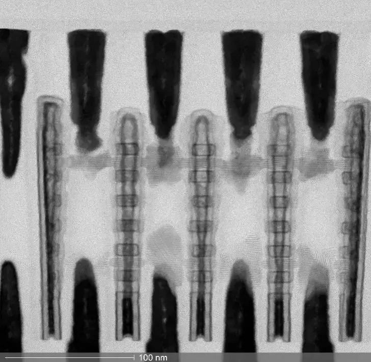
Innovations in Vertical Transistor Stacking
Researchers are accelerating the development of Complementary Field-Effect Transistor (CFET) technology to power future semiconductor nodes. Starting at the A7 logic node, the industry is expected to shift toward this architecture. This transition aims to enable highly efficient 4.5-track standard cells, marking a significant milestone in chip design and performance capabilities.
Breaking news
 Town AI Secures $108 Million Series B, Valued at $1 Billion After $55 M Pre‑Series
 Apple Prepares for Major Product Launch Event on October 28
 Apple Releases Release Candidates for watchOS, tvOS and visionOS 27.2
 Apple Limits iPhone Duo and iPhone 18 Pro Max to Reservation-Only Sales in Japan and South Korea
The advancement relies on two primary research tracks focused on critical integration modules. Engineers are currently perfecting a backside contact module, which is essential for the structural integrity of these devices. By stacking transistors vertically, CFET architectures offer a path to denser, more powerful integrated circuits compared to traditional planar designs.
The core of this research involves developing modular components that allow for complex vertical integration. By refining how contacts are placed on the backside of the wafer, designers can optimize space without sacrificing electrical performance. This modular approach ensures that the manufacturing process remains scalable as transistor sizes continue to shrink toward the A7 node and beyond.
Will CFETs Redefine Future Logic Density?
These improvements are vital for maintaining the pace of Moore’s Law. As traditional horizontal scaling hits physical limitations, vertical stacking provides the necessary room to increase logic density. The current focus remains on ensuring these new modules can be integrated into existing high-volume manufacturing workflows without compromising yield or reliability.
The shift to CFET architectures is not merely an incremental improvement but a fundamental change in how transistors are arranged. By enabling 4.5-track standard cells, this technology allows for a smaller footprint while simultaneously improving power efficiency. These gains are crucial for the next generation of high-performance computing and mobile processors.
Frequently Asked Questions
The industry roadmap indicates that these innovations will be the standard for future logic nodes. As research continues to mature, the focus will shift from experimental modules to full-scale production readiness. This transition will likely define the competitive landscape for chip manufacturers over the coming decade.
What is the primary benefit of CFET technology? CFETs allow for vertical stacking of transistors, which significantly increases logic density. This design enables the use of 4.5-track standard cells, leading to more efficient and powerful microchips.
When will the industry adopt these architectures? The transition toward CFET-based devices is expected to begin at the A7 logic technology node. Research is currently focused on perfecting the necessary integration modules to support this shift.