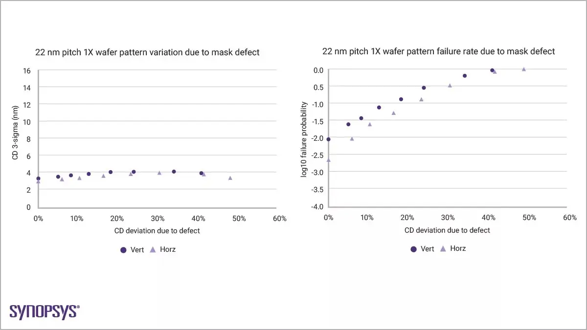
These simulations incorporate real-world data from earlier wafer runs to refine
Semiconductor engineers have long recognized that relying on serial test wafer runs to validate new fabrication processes is inefficient and costly. This challenge has intensified with the advent of deep submicron nodes, where building a new fabrication facility now requires several years and tens of billions of dollars. Each test wafer cycle consumes months and millions in resources, creating significant bottlenecks in technology development. To address this, researchers are turning to advanced optical simulation techniques that can predict silicon behavior years before physical wafers are ever produced. Wafer-validated optical simulation for high-numerical-aperture extreme ultraviolet (EUV) lithography is emerging as a transformative solution. By creating highly accurate digital twins of the lithography process, engineers can model how light interacts with photoresists and substrates under extreme conditions.
Breaking news
 Trump Orders Federal Agencies to Adopt „Super Intelligence” Terminology
 The Silicon Valley Accountability Gap
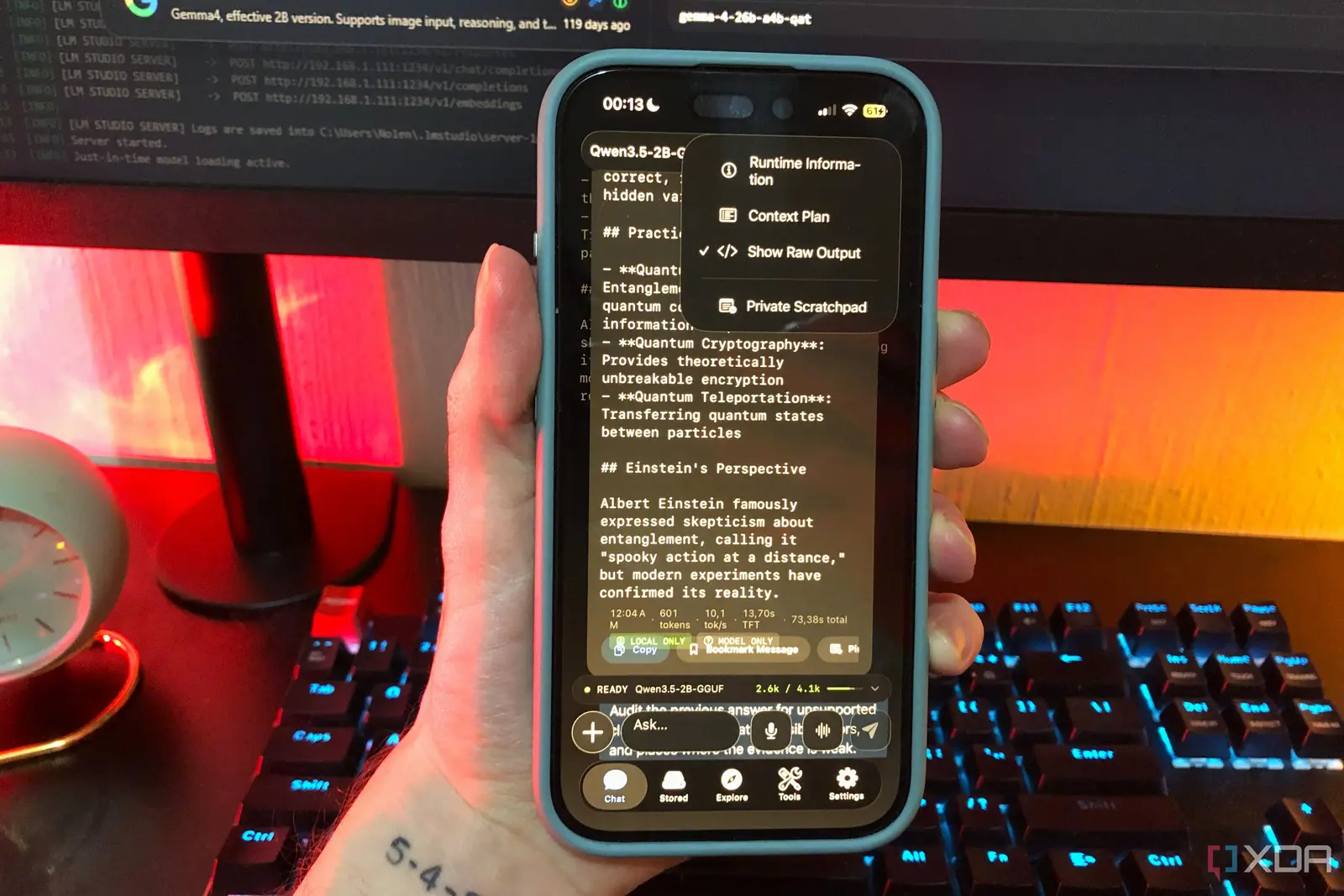 Running a Local AI Model on a Phone Handles Most Chat Prompts
 Google Photos Could Soon Offer a Fresh Start with Ask Photos Feature
These simulations incorporate real-world data from earlier wafer runs to refine their predictive power, allowing teams to identify potential defects, optimize exposure doses, and adjust mask designs virtually. The approach reduces reliance on iterative physical testing, accelerating process development while cutting costs and time-to-market for next-generation chips. How Optical Simulation Mimics Real-World Lithography The simulation framework uses Maxwell’s equations to model light propagation at wavelengths as short as 13.5 nanometers, accounting for complex phenomena like diffraction, polarization, and stochastic effects. Engineers input detailed material properties, scanner specifications, and stack layer data to generate virtual exposures. These outputs are then compared against historical wafer metrology—such as critical dimension measurements and defect maps—to validate accuracy. Over time, the model learns from discrepancies, improving its ability to forecast outcomes for untested process combinations.
This closed-loop validation ensures that simulations remain grounded in
This closed-loop validation ensures that simulations remain grounded in physical reality, not just theoretical ideals. Can Virtual Testing Replace Physical Wafers Entirely? While optical simulation cannot yet fully replace physical validation, it is shifting the paradigm from trial-and-error to predictive engineering. Early adopters report reducing test wafer lots by up to 40% during process development, particularly for high-NA EUV layers where each run is exceptionally expensive. Experts caution that simulations must be continuously updated with new equipment drift data and material variability to maintain fidelity. Still, the ability to run thousands of virtual experiments overnight—something impossible with physical tools—offers unprecedented speed in exploring process windows and resolving yield-limiting issues before they reach the fab. Frequently Asked Questions What makes high-NA EUV lithography particularly challenging for simulation?
High-NA systems use larger aperture angles and more complex optics, increasing optical aberrations and polarization effects that must be precisely modeled to predict resist behavior accurately. How do engineers ensure simulation results match real wafer outcomes? By continuously calibrating models against metrology data from actual wafer runs, adjusting for tool-specific variations and material inconsistencies to maintain predictive validity. Is this approach applicable beyond EUV lithography? Yes, similar optical simulation principles are being adapted for other advanced nodes and technologies, including directed self-assembly and multi-patterning schemes, wherever light-matter interaction plays a critical role.