
How Does The FTCO Workflow Bridge Design And Fabrication?
Researchers have developed a new workflow that bridges the gap between photonic circuit design and real-world fabrication constraints. This approach integrates layout import, 3D process simulation, and GPU-accelerated electromagnetic analysis. The system accounts for physical imperfections that standard simulations ignore.
Breaking news
 AMD FSR 4.1 Lands on RX 6000, Xbox Series, and Ryzen AI Chips
 OpenAI Buys Orchestra Bio to Power Drug Discovery
 Germany’s data center expansion plan hits climate wall
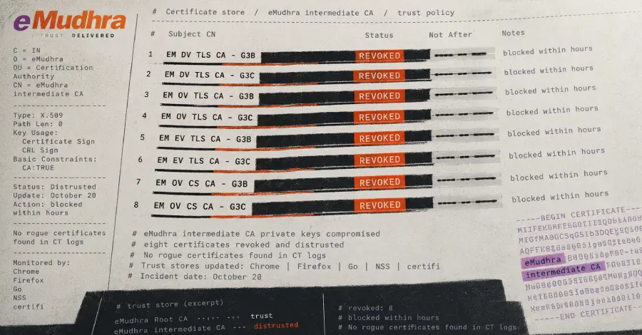 Eight eMudhra CA Keys Compromised, Prompting Emergency Patches Across Browsers
Traditional design tools assume perfect geometry. In reality, manufacturing introduces sidewall angle variations, critical-dimension bias, and line-edge roughness. These factors significantly alter device performance. The new method captures these effects through a digital twin framework.
Why Do Manufacturing Variations Matter For Photonic Devices?
The Fab Technology Co-Optimization workflow begins with importing a GDS layout file. It then runs a 3D process simulation to model how the circuit will actually be manufactured. This step generates a realistic geometric representation of the finished device. The resulting digital twin feeds into GPU-accelerated FDTD simulations. This combination allows designers to predict performance under real fabrication conditions.
Photonic integrated circuits are extremely sensitive to dimensional accuracy. Even nanometer-scale deviations from the as-drawn design shift resonance frequencies and coupling efficiencies. Sidewall angle errors change the effective refractive index. Line-edge roughness scatters light and increases insertion loss. By simulating these effects, engineers can adjust designs before committing to expensive mask fabrication.
What is a digital twin in this context? A digital twin is a virtual replica of the physical device that updates as manufacturing parameters change. It allows continuous validation of design choices against fabrication reality.
Frequently Asked Questions
Why use GPU acceleration for FDTD? FDTD simulations of photonic structures are computationally intensive. GPU acceleration reduces simulation time from hours to minutes, enabling rapid iteration during design.
Can this workflow be applied to other nanophotonic platforms? Yes. The methodology is platform-agnostic and applies to any photonic technology where manufacturing variability impacts performance.