Strategic Timeline and Industry Alignment
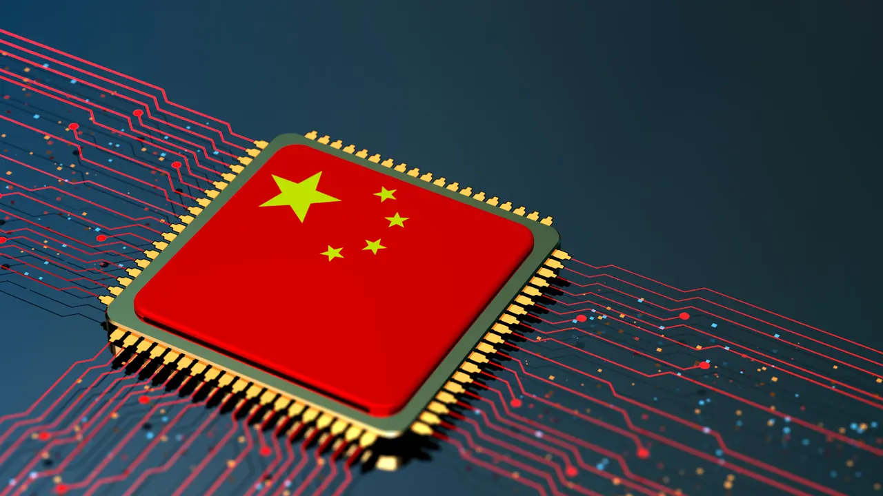
Both companies have signed agreements with ASML Holding to integrate the high-numerical-aperture extreme ultraviolet machines into their fabrication facilities, marking a significant step in the semiconductor industry's race to produce smaller, faster chips. Samsung plans to deploy the technology earlier, while TSMC follows a year later, aligning with their respective roadmaps for advanced process nodes.
Breaking news
 Does the iPhone 18 Pro support longer battery life than the iPhone 17 Pro? Yes, the larger battery and more efficient chip provide roughly 20‑30% more endurance compared to the previous generation
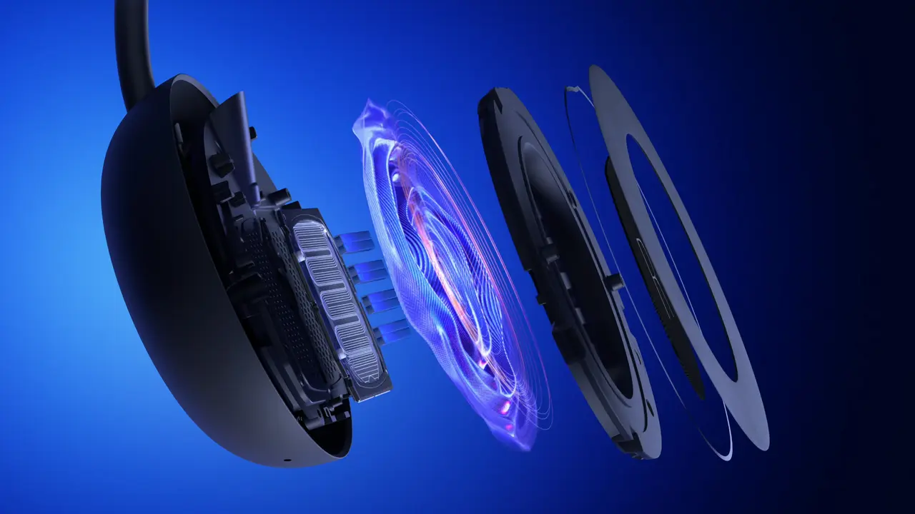 Sony Unveils Two New PlayStation Pulse Headsets With Planar Drivers
 EU Proposes Ban on Social Media for Under‑13s and Restricts Chatbot Use
 Fire Emblem: Fortune’s Weave Captivates Players With Deep Tactical Mastery
The commitments reflect a coordinated effort among the world's leading chipmakers to maintain manufacturing leadership. ASML's High NA EUV systems promise greater precision in etching circuits at sub-3nm scales, essential for future AI and mobile processors. Samsung's earlier adoption could give it an edge in producing cutting-edge image sensors and memory, while TSMC's timeline supports its long-standing partnerships with Apple and NVIDIA. Intel, which previously announced its own High NA EUV plans, continues to lag in mass production but remains committed to the technology.
What Does This Mean for Global Chip Supply Chains?
The staggered rollout may shift dynamics in semiconductor manufacturing, where timing is critical. Samsung's head start could attract new clients seeking early access to advanced nodes, though TSMC's later entry ensures it can incorporate lessons learned. Both companies are investing billions in facility upgrades, with ASML expected to deliver dozens of machines annually starting late this decade.
The broader implications include increased pressure on the global supply chain for EUV components, particularly from Dutch and Japanese suppliers. Analysts predict that only a handful of fabs will initially support High NA EUV, potentially concentrating advanced manufacturing capacity among a few key players.
What is High NA EUV lithography? High NA EUV uses advanced optics to focus light more precisely, enabling chipmakers to print smaller circuit patterns. This allows for transistors at 2nm and below, crucial for next-gen computing performance.
Frequently Asked Questions
Why did Samsung and TSMC commit now? Both companies aim to stay competitive in AI chip manufacturing. Early adoption of High NA EUV ensures they can meet demand for advanced processors while securing long-term supply agreements with ASML.
How will this affect Intel? Intel trails in EUV deployment but has committed to using the machines. Its delayed timeline risks losing market share to Samsung and TSMC, which are already securing capacity and client partnerships.